技術摘要
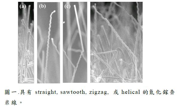
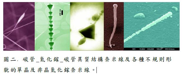
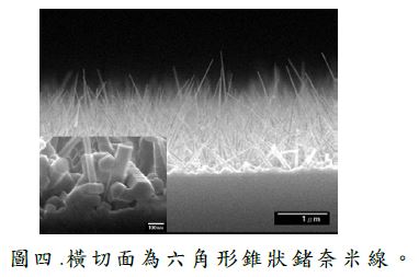
一種合成具有特定功能半導體奈米線結構,進而將具一種或一種以上特定功能半導體奈米線組裝製作成超薄膜片或紙張之製造方法,應用於可捲曲(flexible)半導體電子元件、光電元件、化學感測器、生物感測器、觸控壓力感測器、太陽能電池、熱電晶片、壓電晶片或發電機、電池電極、顯示器、量子電子元件等。此一特定功能奈米線網狀超薄膜片或紙張可以是單獨存在(free standing),也可以與紡織品、紙、塑膠、玻璃、橡膠、高分子聚合物、金屬箔片等可捲曲材料結合,達到輕、薄、耐高溫、熱穩定佳、可捲曲、多功能作用,藉以提升其效能。
A method for manufacturing a semiconductor nano layer structure includes: two substrates are provided; a plurality of semiconductor nanowires are formed on one of the substrates; an absorption surface is formed on the other substrate; one of the substrates is fixed on a cylindrical roller, the cylindrical roller is brought into contact with a surface of the substrate which is stationary and is not fixed on the cylindrical roller, and rolled with a constant velocity and pressure so that the semiconductor nanowires are break, detached, transferred and absorbed, and a semiconductor nano layer structure is formed on the stationary substrate; a de-laminating process is performed to separate the semiconductor nano layer structure from the second substrate; an electric Joule heat welding process is locally performed to bond each of the semiconductor nanowires of the semiconductor nano layer structure or each semiconductor nano layer structure.
現有技術描述、問題及其缺陷
現有製作軟性電子方法為沉積有機高分子薄膜在可撓玻璃或塑膠基板上,此發明則是將無機半導體奈米線組裝製作成超薄膜片或紙張,應用更廣、性能更佳。
產業應用性
可應用於各種光電元件(偵測器、發光二極體、太陽能電池、可攜式顯示器等)、軟性電子元件、電池電極、天線、電磁波過濾器、電磁遮蔽膜、壓力感測器、量子電子元件、單電子電晶體、高敏度化學分子、生物分子感測器、生物晶片、熱電晶片、發電機或具有以上功能組合之物。
本技術發明之目的及達成功效
本案先形成一單獨(Stand-alone)之奈米結構,可自由應用此單獨成形之奈米結構進行製程上之調配,因此本案之製程靈活度較高。
圖片A
圖片B
圖片C
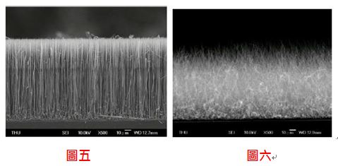
圖五:具p-i-n結構之筆直豎立矽奈米線陣列。 圖六:具p-i-n結構之不規則矽奈米線陣列。